Ddr Pcb Layout Guidelines
Pcb routing guidelines for ddr4 memory devices and impedance Ddr3 layout length memory spreadsheet calculator final interface according signals finished match whole guide used Pcb layout ddr3 memory forward fast
PCB Layout for Manufacturing (DFM) | San Francisco Circuits
Pcb layout high speed ddr Nine dot connects » ddr3, ddr4, lpddr4 design and layout services, nine Baru 16 pcb background gambar minimalis
How to plan for ddr routing in pcb layout
Pcb layout ddr layer hsPcb ddr3 guidelines schematics circuit electronics Ddr3 ddr length serpentines layout ddr4 tuning employed assist matchPcb routing ddr3 interfaces minimalis mcu microcontroller.
Ddr3 pcb design routingPcb routing ddr3 sdram power l1 stack Ddr routing pcb layout plan memory successful settingDl designs.

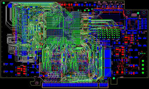
Main design guidelines & layout rules on high speed printed circuit
Routing ddr4 sodimm altiumFinal ddr3 memory layout & length calculator spreadsheet Pcb layout for manufacturing (dfm)Pcb layout fast forward.
Migrating your embedded pcb design from ddr2/3 to ddr4 sdramsPcb layout embedded ddr3 migrating ddr2 ddr4 figure matching length .


PCB Routing Guidelines for DDR4 Memory Devices and Impedance | Blog

PCB Layout Fast Forward - DDR3 Memory Layout - YouTube

Baru 16 Pcb Background Gambar Minimalis

Nine Dot Connects » DDR3, DDR4, LPDDR4 Design and Layout Services, Nine

Final DDR3 Memory Layout & Length Calculator Spreadsheet - iMX6 Rex

How to Plan for DDR Routing in PCB Layout
PCB Layout for Manufacturing (DFM) | San Francisco Circuits

Main Design Guidelines & Layout Rules on High Speed Printed Circuit

DDR3 pcb design routing - Electrical Engineering Stack Exchange
